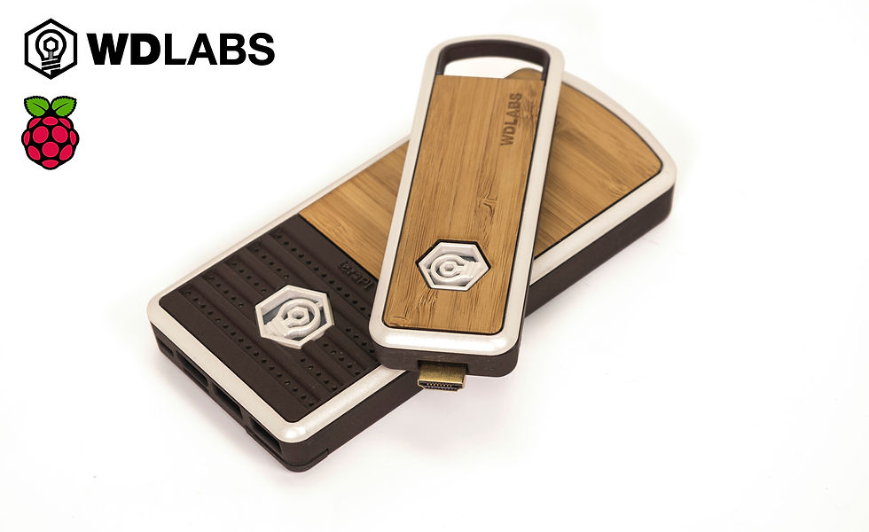
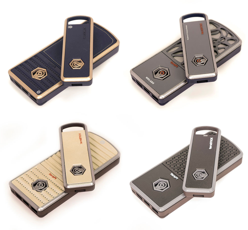
WD Labs had a few ideas centered around the Pi compute module so we created a few test PCBs. Then we contacted Eben Upton and he said he would love to stop by in 2 weeks when in town visiting Broadcom. WD Labs scientists created the pcbs - I designed and created the enclosures. This was the process and the 10 day results.
Phase I
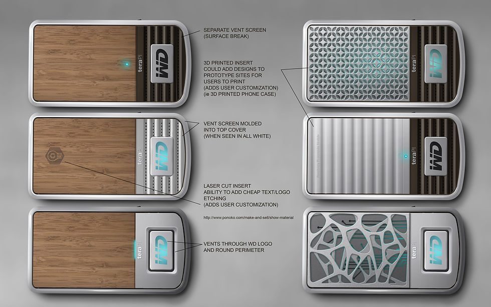
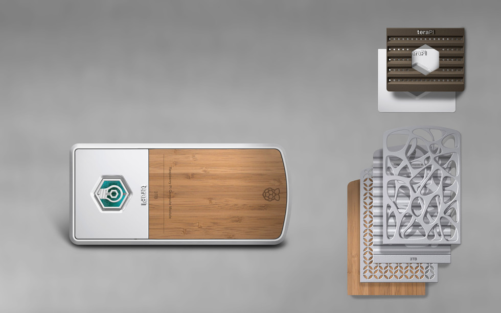
Quick one day exploration exercise to provide solid design families to develop into physical shells for our prototype compute module pcbs.


PROJECT INVOLVEMENT
Industrial Design
Product Development
Photo Realistic Renderings
Mechanical Engineering / Drawings / Solidworks
3D Prints
Color Studies
Model Maker
Phase II
The refinement of chosen design and packaging exploration


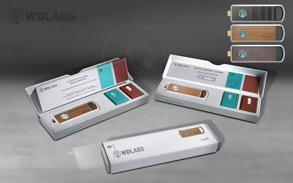
Prototypes
Additional color and texture exploration for the the 8 prototype sets that we created
Ryan
Comments